How a computer works (Part 1)

Hello dear interwebs,

I just found this blog post that I wrote in 2013… Never finished it, never published it… I’ve updated it slightly (in blue) and then finished writing it so I can finally publish it 6 years later… here it goes :


I was recently thinking about how computers work and I know a lot of you reading me would enjoy knowing more about the details of it, so I decided to write another educational post (kind of like the ECDSA post a few months years ago).

Once more, I need to write a disclaimer saying that this is a relatively simple explanation, I will try to make it easy to understand, but it means there might be some inaccuracies, or incomplete information, so don’t be surprised if you see something wrong, just let me know, it might be my mistake, or it might have been on purpose for the sake of simplicity.

Binary data

First, let’s start with the basics. Many of you will know what binary data is and how it works, but I don’t think everyone does, so I’ll try to explain it briefly. If you already know what this is, maybe you can skip this section.

So, ‘binary‘ is just a way to represent numbers, as you probably know, we use the ‘decimal’ base (decimal means 10), that’s probably due to the fact that human beings have 10 fingers (also known as digits in the English language, not a coincidence). This means that we use 10 ‘digits’ in our ‘alphabet of numbers’.. just like we have 26 letters in the alphabet and putting them together forms words, we do the same with numbers, by using the 10 digits (0 to 9) and putting them together to form numbers. A zero can be written as ‘0’ or as ‘0000000’, and when you start to increment it (counting), once you reach 9, your first digit goes back to 0, and the second digit is increment from 0 to 1, giving you 10 (or 000000010).
Let’s take the random number 1234, that can be written as :

1 * 1000 + 2 * 100 + 3 * 10 + 4 * 1 = 1234.

Note also that 100 is 10 * 10 or 10 to the power of 2 (10^2) and 1000 is 10 * 10 * 10 or 10 to the power of 3 (10^3) and also note that 10 is 10 to the power of 1 (10^1), and 1 is 10 to the power of 0 (10^0)..
So for a random number with digits xyz, it can be written as :

x * 10^2 + y * 10^1 + z * 10^0 

It’s actually quite simple, a decimal base for numbers simply means that each digit can have 10 different values, and when you reach the maximum value, you go back to zero and increment the next digit to its left (after 9, it’s 10), and the total value is the addition of each digit multiplied by your base (10) exponent the position of the digit in the number.

Binary data is the exact same thing, but it uses base 2, which means that there are 2 possible digit values (0 and 1), and you use ‘2’ as the multiplier, in other words, a random binary number xyz is the same as :

x * 2^2 + y * 2^1 + z * 2^0, or
x * 4 + y * 2 + z * 1.

This means that the binary value 010011101 is the same as the decimal value 2 *1 + 0 * 2 + 1*4 + 1 * 8 + 1 *16 + 0 *32 + 0 * 64 + 1 * 128 + 0 *256 = 157.. 

An easy way for me to read binary values is to simply assign a value to each digit and add them if the value is 1. Those values are of course the 2 exponents, so : 1, 2, 4, 8, 16, 32, 64, 128, 256, 512, 1024, etc.. in other words, for the previous example of 010011101 :

   0   –   1  –   0 –  0  –  1 –  1 – 1 – 0 – 1
256 – 128 – 64 – 32 – 16 – 8 – 4 – 2 – 1

So I add (from right to left), 1 + 4+ 8 + 16 + 128… which gives me 157.

When we talk about binary, we use the term ‘bit’ to represent one ‘digit’ of the number, and when we have 8 bits, we call them one ‘byte’. So one byte can have 256 values, from 0 to 255 (128+64+32+16+8+4+2+1 = 255).

That’s pretty much all you need to know about binary data… let’s move on now!

Why do computers use binary ?

The reason is simple: computers work using electricity (duh!) šŸ™‚

So, how can a computer do all of the stuff it does just by using electricity? Well, it’s simple, it uses electricity to represent binary data. If there is electricity on the wire, it’s a 1, if there is no electricity, then it’s 0… by simply controlling if there should be some electrical current on a wire or not, and how that electricity changes over time, it’s able to represent numbers and any other data it wants by simply using that binary representation, and it uses that in order to accomplish a lot of stuff.. A number can be used to represent anything, depending on how the computer decides to interpret that value… and so it can an actual number, or a character, or a pixel, or even code,  let’s see what it does with it.

Assembly code

You’ve all probably heard of people talking about “assembly code”… the assembly code, also known as “machine code”, is just some binary data that the CPU (the processor) can understand. The assembly is just a way to tell the computer what to do, it’s basically just giving instructions to the computer for it to accomplish, depending on what value it has. Like I said above, a number can represent anything, so let’s create some fake assembly code, we’ll just assign an ‘instruction’ to some numbers :

1 = add
2 = substract
3 = multiply
4 = divide
5 = copy
etc…

When the computer reads the assembly code, if it seems a ‘4’, it will divide, if it sees ‘1’, it will add, etc… For now, I won’t explain what it adds, or where it stores it, or how it does it, etc.. I’ll leave that for a potential part 2 of this article.

I’ve actually written an introduction to assembly code and reverse engineering a few years after I wrote this article, which you can read here.

Transistors

Oh, the transistors, everyone probably heard that word but noone really knows what it means… all we know is that computers are full of transistors and that’s how it functions…

Well, a transistor is simply a sort of electronic switch, like your door bell, for example. It has two wires, and a button, if you push the button, the two wires are connected together and the electricity flows through them, if you release the button, the two wires are disconnected, and the bell stops ringing. That’s the whole basis of how a computer works, transistors are indeed at the heart of its functioning, and I will explain how and why.

So, like I said, a transistor is like a switch, but it doesn’t use a button, it just uses a third wire. Let’s say you have a transistor with wires A and B and S. when there is electricity flowing through the wire S, then A and B are connected, if there is no electricity flowing through S, then A and B are disconnected.

By using these transistors, we can build some slightly more complicated, and very useful, components which is what the computer really uses. These are called “logic gates”, and that’s what I want to talk about in this article, but first, I want to explain how those logic gates work.

Logic gates

So, what is a logic gate? A logic gate is an electrical component whose output is influenced by its input, there are 3 major logic gates, the AND, the OR, and the NOT. Let’s start with the NOT since it’s the most simple… it has an entry “A” and an output “Z”, if the value of A is 0, then the output Z will have a value of 1, if the value of A is 1, then the output Z will be 0. Now you notice, I said “0” and “1”, instead of “electricity flowing through the wire” like I was saying before.. simply because, as I explained before, the computer uses binary data and it’s represented by whether or not electricity is flowing. When we talk in terms of logic gates, we talk in terms of binary input and output, but it is indeed the same thing as saying that electricity flows through it.

Here’s the Input/Output table for the NOT gate (Called the Truth Table): 

Input AOutput Z
01
10

Now, the AND gate should be obvious, it has two inputs A, and B, and one output Z, if both the input A and B are 1, then the output Z is 1, if one of the inputs or both of them are 0, then the output Z is 0. The same logic can be applied to the OR gate, if at least one of its input A or B is 1, then the output Z is 1, if both inputs A and B are 0, then the output is 0.

Here are both of their I/O tables :

ANDOR
ABOutput ZABOutput Z
000000
010011
100101
111111

There is a fourth logic gate called a XOR, or “Exclusive OR”, which acts a bit differently, in its case, if A or B is 1 but NOT both at the same time, then its output Z is 1, otherwise, it’s 0. The XOR gate can easily be created by mixing together a couple of AND and OR and NOT gates in order to achieve the same result.

ABOutput Z
000
011
101
110

From these logic gates, there are some others than can be created, the NAND and NOR gates, which are simply the same as “NOT AND” and “NOT OR”, the output Z has the opposite value of what it should be with the AND and OR gates respectively, and they can be created by connecting the Z output of the AND (or the OR) to the A input of the NOT. They are still considered as logic gates because they can be created into a single component using less transistors than if we used both the AND + NOT components linked together… but that’s not particularly important.

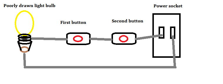
Let’s see how you can create an AND gate using transistors… Don’t forget that these are electrical components, which means they need power, like any of your electrical devices, so truly an AND gate will have 5 entries (known as ‘pins’), one VCC (power), one ground (represents 0V), the A and B inputs and the Z output, you can imagine it as being one box that you plug into your wall power socket, and it has two buttons and one light bulb, if you press both buttons, the light bulb goes on.

So the simple solution would be to connect your light bulb’s ground to the ground pin, and the light bulb’s power connector to one side of the first button, connect the two buttons together and connect the other wire of the second button to the power cord. This way, when you press both buttons, the power flows through the light bulb since the connection is made.. Let me show you my awesome skills in using Paint :

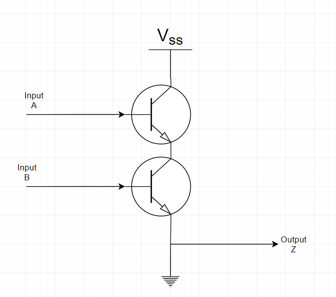
Thinking about it in terms of transistors, you would connect the Z output to one end of a transistor, connect the other end to one end of another transistor, and connect that other end to the power, then you can connect your A input to the ‘S’ pin of one transistor, and your B input to the ‘S’ pin of the second transistor… Here’s what a properly drawn (just means I didn’t use Paint this time, but it’s still a simplification) electrical schema would look like :

AND Gate

I will leave it to you as an exercise to try and figure out how to connect transistors together in order to create an OR, XOR and NOT gate.

Now, that’s about as far as I got when writing this in 2013, and I don’t remember all I had planned to write, but I think that the following section is going to be interesting.. it was one of the most interesting things I had to do at university. I won’t use blue for the rest, but whatever is written below was written in 2019.

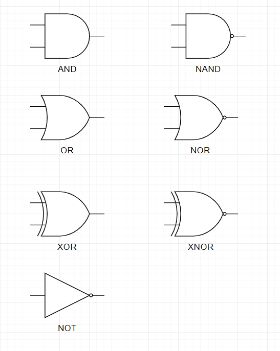
One last thing I want to say about logic gates before we get started is that, this is how they are represented in schematics :

Logic gates

A simple adder

The task we will be doing now is to create a simple adder. An adder is a small electrical circuit which does an addition and nothing else. A simple adder is the same thing but it only does it for single digit numbers (which means a single bit, in the binary world). Get ready, we’re gong to kick it up a notch…

The first step will be to create the Truth Table for our adder. If we add 0 + 0, that gives us 0, that’s obvious.. if we add 1 + 0 that gives us 1, same thing for 0 + 1 of course, but then what do we do with 1 + 1 ? That gives us 10 (which is 2 in binary), but we’re working with a single bit, so ? So it’s simple, the answer is 0 and we have a carry.

Here’s the truth table for our adder which takes two inputs A and B and gives the sum S as its output :

ABS
000
011
101
110

Does this look familiar? Yes, exactly, it’s the same truth table as the XOR table above… So a simple XOR logic gate is already doing an addition for us!

Let’s make it a little more complicated, what if our adder had two outputs, the sum S and the carry value C. We get this truth table :

A (Input)B (Input)C (Output)S (Output)
0000
0101
1001
1110

If we just look at the C column, it looks very similar to the truth table of the AND gate.. So the Carry bit is the result of an AND gate. That sounds really simple, let’s create a circuit with that :

Half Adder

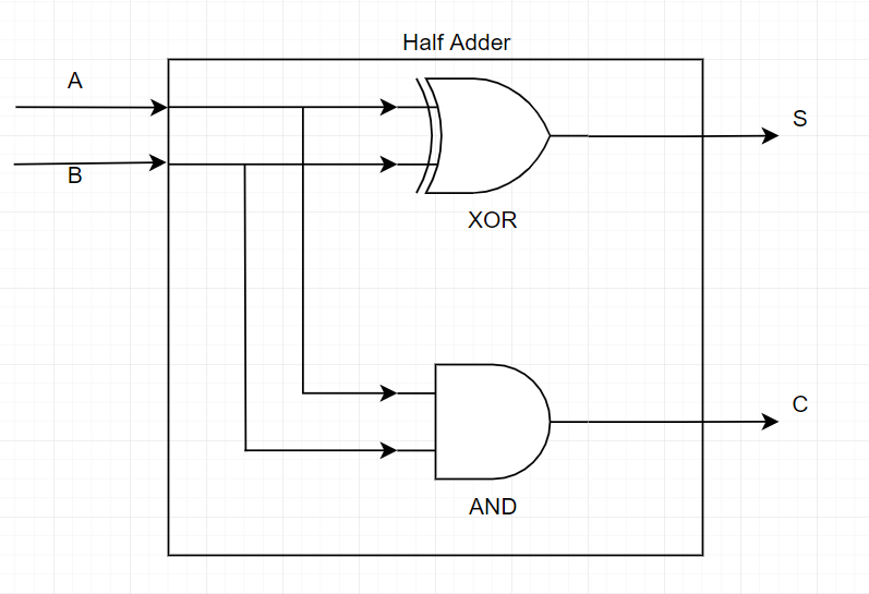
That looks simple enough, right? Well, it is, but it’s also pretty useless, right? What can you do with just 1 bit additions… Also, the one with the most observation, may have noticed that the circuit above was titled ‘Half adder’ and wondering what I mean by ‘half adder’.. well, it just means that it doesn’t take into account a possible carry from a previous operation. A full adder will be the same thing, but it also takes a third input ‘CIN’ (for Carry-In) to do the addition.

If we were to do a full adder, we’d need 3 inputs, and here is the truth table for it (try to write it yourselves before looking, would be interesting to see if you get it right) :

A (Input)B (Input)CIN (Input)COUT (Output)S (Output)
00000
00101
01001
01110
10001
10110
11010
11111

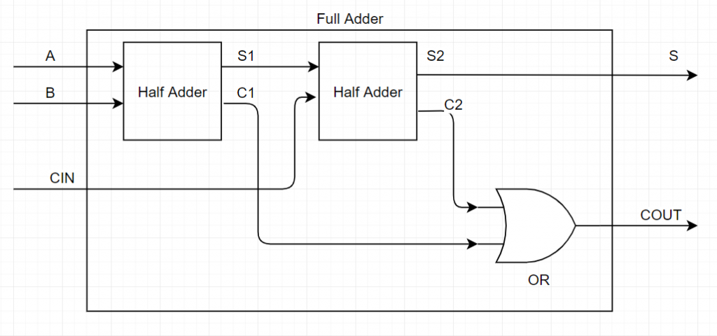
Do you want to try and figure out what logic gates to use to build such a circuit ? There are equations you can use to determine the most optimal gates for each output based on the inputs and the truth table, but I’m not going to show you that here. Instead if you filled the table yourself or looked at it enough to understand it, or just use your brain’s logic, you would have figured out that a full adder is basically just doing the sum of the 3 inputs, so it’s a 3 bit addition, so ‘A + B + CIN’ or ‘(A + B) + CIN’, yes.. it can be built using two half adder. Let’s do that now :

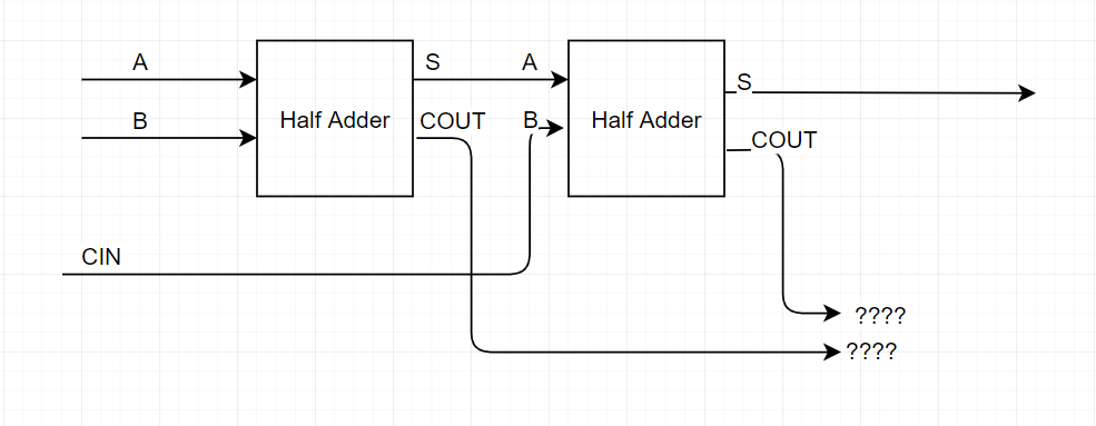
Well.. we have a problem, once we add the partial sum S from the first half adder and add the carry CIN to it, we end up with two carry values, one from each half adder, plus our sum. Are we back to square one having to add 3 bits again? How do we determine our own sum and carry output? Well, let’s do a truth table using the partial sum S1 and carry C1 with the second operation’s sum S2 and carry C2.

Note that we know that the sum value S1 will always be 0 if C1 is 1, and S2 will always be 0 if C2 is 1 (see the half adder’s truth table above). But also that the carry C2 can never be 1 if both CIN and S1 are not 1. Therefore, we can only put a 1 in the C2 column if S1 is also 1, and we can only put 1 on the S1 or S2 columns if C1 or C2 respectively are 0. We also know that if S1 is 1, then we can’t have both S2 and C2 set to 0.

A (Input)B (Input)CIN (Input)S1C1S2C2COUT (Output)S (Output)
000000000
001001001
110010010
111011011
1
0
0
1
1
1
100110
1
0
0
1
0
0
101001

Looking at the table, we can see that our output S is always the same value as S2, and that our carry COUT is 1 if any of the two operations caused a carry, in other words, if we clear out the columns we don’t care about in the previous table, it’s looking like this :

C1C2COUT
000
101
011

That looks like a simple OR gate, so let’s do that and we get our full adder :

Full Adder using 2 half adders and a OR gate

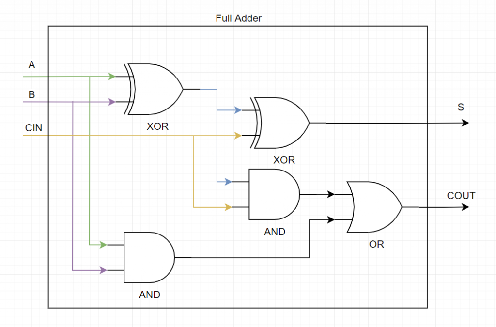
Or if we ignore the half adder blocks and just show the logic gates in use, this is the result :

Full adder

So, you know how to do additions using logic circuits and you’re probably wondering how that’s useful and how that helps you better understand how a computer works. Well, the reason the full adder is so cool is that you can chain it up. So here’s a very simple 4 bit adder :

4 bit adder

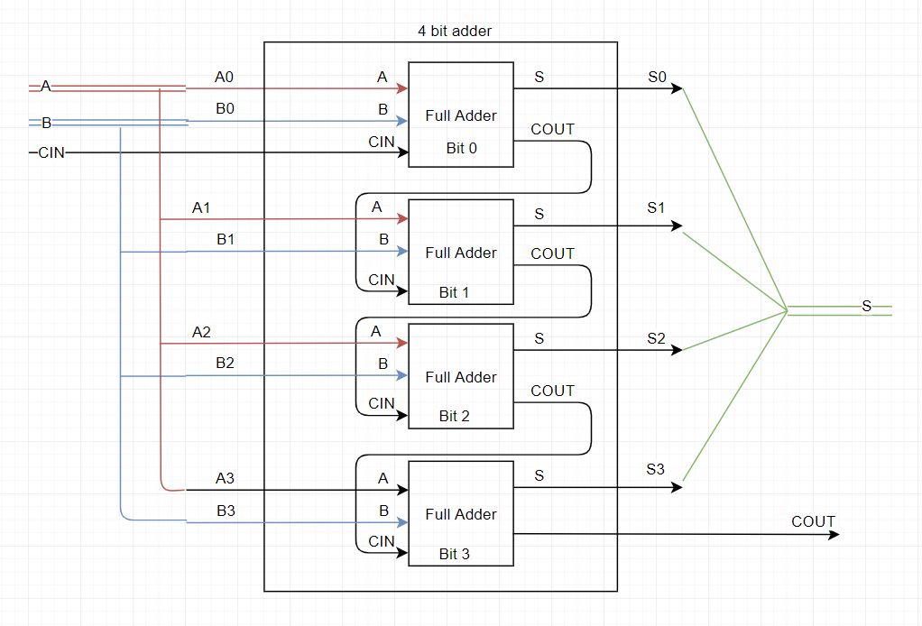
It’s not so bad, right? you have a 4 bit value (0 to 15) A and another 4 bit value B, you can add it and get your sum S on 4 bits with a carry. You can do this until you get to 32 bits, which is a full integer on 32 bit systems.

By having a 32 bit adder, and a substracter and divider and multiplier and all sorts of other small components like that, using logic gates which use transistors, you end up with a bigger block called the ALU (Arithmetic Logic Unit) and with even more complex circuits, you end up with a CPU (Central Processing Unit) which is what runs your entire computer’s logic.

Multiplexers and demultiplexers

I’m not going to get into multiplexers (mux) and demultiplexers (demux) too much, but I want to explain the basic concept. A multiplexer will select one input based on a selector and put it into its output. Let’s assume we have 8 input lines, I0, I1, I2, … I7, and one output Z.. we want to connect Z to one of those input lines, so we use a 8-to-1 multiplexer and use a 3 bit selector (since 3 bits can hold values 000b (0 in decimal) to 111b (7 in decimal) which is enough for our 8 inputs). Based on the value of the selector, the output will be connected to the appropriate input. Sounds simple enough right ?

You can read more about them on this wikipedia page and here’s a drawing taken from that page that shows the logic gates used to construct a 4 to 1 mux :

4 to 1 mux

A demuxer is the opposite. It receives one input and a selector and outputs it one of its numerous outputs. So let’s say a demuxer has 8 outputs, if the selector has value 5, then the 5th output will be connected with the input of the demuxer.

Why I’m explaining all of this? Because the computer is a big muxer/demuxer and that’s how it executes code. You remember when I said that a transistor actually has 5 pins? the 2 inputs A and B, the output Z but also a power input and a ground input to actually power it ? Well, since logic gates are made of transistors, they also need to be connected to both a power source and ground (how would you expect a NOT to output a 1 (which is 5 Volts) if it receives 0 as inputs (which is 0 volts).. we’re not creating energy out of thin air! So yes, these circuit diagrams are always simplified, but you can always assume that every transistor, every logic gate, and every half/full-adder block, multiplier block, ALU, CPU, etc.. will have a 5V power and ground pin going into it.

Your CPU (or ALU in the example below) receives an instruction and needs to ‘decide’ what to do, so here’s how it does it :

  • Connect all your inputs to every instruction block you have, so your A and B inputs will go into the addition block, substraction block, multiplication block, etc…
  • At the output, use a gigantic OR gate (chaining multiple OR gates one to the other) to OR the output of all of your instruction blocks and put that as your single output.
  • Use a demuxer where the instruction you received is the selector of the demuxer, the input is connected to the 5V power input and each output of the demuxer is connected to the 5V power input of each of your blocks.
  • When you receive an instruction, only one of the blocks will be active because only one of those blocks will receive power.

And that’s how you make your CPU decide on what to do when it receives an instruction šŸ™‚

SR Latch

This is mostly just for fun, but if you’re wondering what else can be done with transistors and logic gates, how about memory ? Yes, a simple 1 bit memory component can be created using a few logic gates, they are called flip flops. A simple one is called an SR Latch. the ‘SR’ is because of its inputs. S for ‘set’ (set the memory value to 1) and ‘R’ for Reset (set the memory value to 0). Can you figure out how to create a small block with only two logic gates which can act as memory ? Here’s a hint, you only need 2 NORs… how would you connect them in such a way that it remembers the last value you set/reset it to ?

Well, you can read more about flip flops on wikipedia here and here’s how it can be done :

SR Flip-Flop

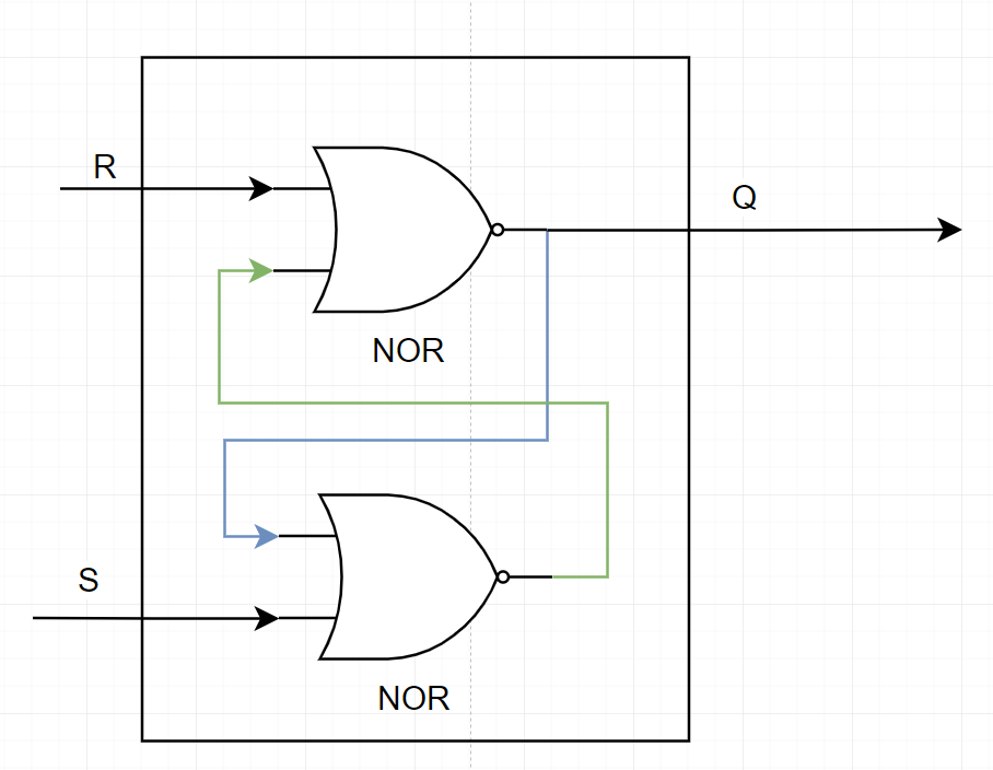
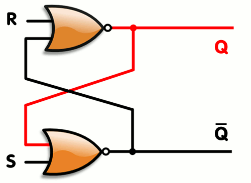
As you can see, by connecting the two gates’s output as input to their companion, you create memory.. One you set 1 to the S value, the bottom NOR gate will output a 0, which will cause the top gate to output a 1 (remember, a NOR will like an OR gate with a NOT at the end, so it will output a 0 whenever an input is 1 and will output 1 when both inputs are 0). When the top gate is outputting 1, this causes the bottom gate to keep receiving a 1 on its inputs even if S stops being set. When setting R to 1, it will force the top gate to output 0, which does the same thing in reverse… Here’s a simple animation that shows how it works (copied from its wikipedia article) :

Animation of how an SR latch functions

Conclusion

You can build from that, from the simple “electricity means 1 and no electricity means 0”, into using transistors (basically electric push buttons) to build the AND, OR, NOT, XOR logic gates to building a more complex logical block such as an adder or a demuxer to building an even more complex processing unit such as an ALU using multiple blocks and a demuxer to interpret instructions it receives to building the extremely complex CPU which handles billions of instructions per second in order to do what we want it to do.

The transistors let us create memory, and computers and basically any electronics device will have transistors in them. According to the wikipedia page for transistor count, a recent CPU has about 7 billion transistors. The iPhone 11 Pro has 8.5 billion, and the PS3’s Cell processor had 250 million transistors… And to think that at some point in the past, a single transistor was as big as a light bulb…

I hope this was interesting and entertaining and mostly educational. I’ve obviously gone very quickly from the very basic to the very complex, but I hope you were all able to follow regardless and even if you don’t understand all of it, you get the broad strokes and understand better how a computer works.

Intel FSP reverse engineering: finding the real entry point!

DISCLAIMER: This post was originally posted on Puri.sm‘s blog but then taken down after they received a letter from Intel requesting the article be removed as it contained information about reverse engineering the FSP which was against their License. I am putting this article back up again on my personal blog for the following reasons :

  • Their current license only prohibits the reverse engineering with regards to ‘Redistribution’, and since I am not working for Purism anymore, I am not involved with redistribution of any of their binaries and therefore it does not affect me.
  • The files I had originally worked on were cloned from this specific commit on their repository which had a BSD style license which did not prevent any reverse engineering (but I do know that a more restrictive license was added in a subsequent commit 30 minutes later, but it wouldn’t change the fact that the FSP in that specific branch is using the BSD license and the ‘license change’ wouldn’t be considered retroactive).
  • Since I live in Canada, Reverse Engineering is allowed when it comes to security or interoperability, which is the case here. I know that this is more of a license issue than a copyright violation issue (where Canadian law would apply), but I don’t see why someone could revoke my right to do security research by invoking a license breach.
  • The reverse engineering and security research that has been done in recent years by other companies or individuals (most notably PT Research or Peter Bosch) has far surpassed what I have written in this article, and this article is a lot more educational and along the lines of my previous Introduction to Reverse Engineering article than one about secrets hidden in the assembly code. I think that whatever damage Intel might think it does is extremely minimal compared to other existing projects.
  • The article is and has always been available on the web archive, so it wasn’t ever really taken down from the internet, whether to link to my blog or to the web archive when people mention this article would make no actual difference. I think the important part is that it is not hosted on purism’s website since they are a laptop manufacturer and therefore a distributor of the FSP within their products.

For the above listed reasons, among others, I am releasing this article to the public again. I have also gone through it to remove a particularly long code snippet which was not required for understanding and made sure that any other screenshots I’ve had would fall well within the fair use clause.


After attending 34C3 in Leipzig at the end of December 2017, in which we (Zlatan and me) met with some of you, and had a lot of fun, I took some time off to travel Europe and fall victim to the horrible Influenza virus that so many people caught this year. After a couple more weeks of bed rest, I continued my saga in trying to find theĀ realĀ entry point of the Intel FSP-S module.

WARNING: This post will beĀ veryĀ technical, and even if you are a technical person, you will probably need to have read my previous ā€œPrimer guideā€ blog post in order to be able to follow most of it. If however, youā€™re not a technical person, donā€™t worry, hereā€™s the non-technical executive summary:

  • I made some good progress in reverse engineering both the FSP-S and FSP-M and Iā€™m very happy with it so far
  • Unfortunately, all the code Iā€™ve seen so far has been about setting up the FSP itself, so I havenā€™t actually been able to start reverse engineering the actual Silicon initialization code.
  • This blog post is about finding the ā€œreal entry pointā€, the real silicon initialization code and Iā€™ve been jumping through a lot of hoops in how the FSP initializes itself in an attempt to find where it actually does start the initialization code and I believe Iā€™m very close to finding it.
  • Progress is good and still ongoing, and the task will be done at some point, so stay patient as you have been so far.
  • This post is mostly about going step by step over the process of reverse engineering that Iā€™ve done so far. It helps you follow along on the progress, helps some of you learn how itā€™s done and what happens behind the scenes.

Diving back into the depths

If you remember, in myĀ primer to reverse engineering the FSP, I said the following :

ā€œIā€™ve finished reverse engineering the FSP-S entry codeā€”from the entry point (FspSiliconInit) all the way to the end of the function and all the subfunctions that it calls. This only represents 9 functions however, and about 115 lines of C code; I havenā€™t yet fully figured out where exactly itā€™s going in order to execute the rest of the code. What happens is that the last function it calls (it actually jumps into it) grabs a variable from some area in memory, and within that variable, it will copy a value into the ESP, thus replacing our stack pointer, and then it does a ā€˜RETNā€™ā€¦ which means that itā€™s not actually returning to the function that called it (coreboot), itā€™s returningā€¦ somewhere, depending on what the new stack contains, but I donā€™t know where (or how) this new stack is created, so I need to track it down in order to find what the return address is, find where the RETN is returning us into, so I can unlock plenty of new functions and continue reverse engineering this.ā€

Diving Deeper

Today, we will examine what happens in more details. Get ready for the technical part now, because weā€™re going to dive right back in, and weā€™re going to go pretty deep as I walk you through the steps I took to reverse engineer that portion of the code to figure out what happens. Iā€™ll go pretty fast over things like ā€œlook at this ASM function, this is what it doesā€ because you donā€™t need the details; Iā€™ll mostly explain the weird/unusual/non-straightforward things.

First, a little preface: there are two FSP files, the FSP-M and FSP-S. The FSP-M contains the functions for the memory initialization and the FSP-S contains the functions for the silicon initialization. Coreboot will run the MemoryInit from FSP-M during its romstage, then once the RAM is initialized, it will start its ramstage in which it will run the SiliconInit function from the FSP-S file.

The FSP-S file is loaded into memory by coreboot, then the address of the ā€˜SiliconInitā€˜ function is retrieved from the FSP-S file header and coreboot calls that function. That function is pretty simple, it just calls the ā€˜fsp_init_entryā€˜ function (thatā€™s how I called it). Actually, all of the FSP entry point functions will call this same fsp_init_entry() but will set %eax to a different value each time, to represent which FSP entry point function was called. See for yourselves:

Note that in the FSP-S file, the ā€˜jmp fsp_memory_initā€˜ (in the lower-right corner) is replaced with ā€˜jmp infinite_loopā€˜ instead. This screenshot was actually taken from the FSP-M file, which is why it shows ā€œjmp fsp_memory_initā€œ.

So, each of the entry points in the various FSP images (on the left, I showed entry points for both FSP-S and FSP-M files) will call fsp_init_entry which will call validate_parameters() and then if the %eax register is 3 (youā€™ll notice thatā€™s the value set by memory_init_entry), it will call fsp_memory_init, otherwise it will jump into switch_stack_and_run (after calling gst_fsp_info_header, youā€™ll see why below). All that the switch_stack_and_run() function does is to replace the stack pointer (first storing all of the registers into it and replacing all the register values from ones taken from the new stack), then finally return. See for yourselves:

It might look complicated, but itā€™s not that much:

  1. it does a bunch of ā€˜pushā€˜, the first is to push %eax, which is the return value from the previous ā€œcallĀ get_fsp_info_headerā€ call in theĀ fsp_init_entryĀ function above,
  2. then it calls ā€˜pushfā€˜ which pushes the EFLAGS register,
  3. then ā€œcliā€ will disable interrupts (this is to avoid having some interrupt triggered and change things from under our noses),
  4. then ā€˜pushaā€˜ which will push all of the registers into the stack,
  5. then we subtract 8 bytes from the stack, basically allocating 8 bytes,
  6. then calling ā€˜sidtā€˜ which is ā€œStore Interrupt Descriptor Tableā€.
  7. Finally it calls ā€˜save_fspd_stackā€˜ and it gives it the %esp (stack pointer) as argument. That function will store that argument into offset 8 of the address stored in 0xFED00148ā€¦ but since I already reversed that, letā€™s make it easier for you and just say that it stored the argument in the StackPointer field (offset 0x08) of the FSPD data structure,
  8. then return in %eax the previous value that was stored there.
  9. switch_stack_and_runĀ will store the returned address into %esp, effectively replacing the entire stack,
  10. then it will proceed toĀ popĀ back all the registers, flags, IDT back into their respective places,
  11. then return which will make us return not into theĀ fsp_init_entryĀ function (nor to coreboot since fsp_init_entry actually did a ā€˜jmpā€˜, not a ā€˜callā€˜), but rather it returns to whatever was the return address of the calling function from the new stack pointer.

This is what I explained in my previous blog post (which I quoted at the beginning of this post).

To make things easier to visualize for you, hereā€™s a description of the stack contents (as an IDA structure):

In the picture above: youā€™ll notice that of course, the top of the stack contains the last thing that was pushed into it, and the ā€˜ddā€™ means ā€˜data double wordā€™ (4 bytes) and ā€˜dwā€™ means ā€˜data wordā€™ (2 bytes) so youā€™ll see the ā€˜idt_ā€™ values at the top of the stack represent 8 bytes (2 + 4+ 2) because as the ā€˜sidtā€˜ instruction describes, the IDT is made up of 6 bytes, the limit (2 bytes) and the base address (4 bytes). You may also notice the ā€˜first_argument_on_stackā€˜, thatā€™s because theĀ silicon_initĀ was called with an argument (UPD configuration structure) and that was initially on the stack and still is on the stack when the stack exchange occurs.

If you want to see the C code equivalent that I wrote when reverse engineering these functions, head over to the newĀ git repositoryĀ I created for this project. This code is common to both FSP-S and FSP-M and so itā€™s available in theĀ fsp_common.cĀ file.


Iā€™m FED00148 up

So now, the big question! I had no idea whatā€™s in this ā€œ0xFED00148ā€ address (the one you saw as ā€˜ds:FSPDā€™ above) or who sets its content, or what it contains. I eventually figured out itā€™s the ā€œFSP DATAā€ structure and I know what some of its fields are (such as the Stored StackPointer at offset 8), but at first, I had no idea, so hereā€™s what I did: I dumped the content of the 0xFED00148 address from coreboot prior to calling SiliconInit, that gave me the address of the FSPD structure and at offset 8, I found the new stack pointer that the FSP-S will use, and from there, I manually popped the values until I found the new return address.

Thanks to my previous StackContents structure, we already know that the return address is at offset 0x30 in the saved stack, so in the above coreboot console output, we see the return address value is 0xffcd7681 (what you see as ā€œ81 76 cd ffā€ above, because x86 stores data inĀ Little-Endian, that means the bytes are read right to left), and that doesnā€™t match anything in the FSP-S since we can see that theĀ silicon_initĀ function is at 0x6f9091da and offset 0xffcd7681 is way beyond the boundaries of the FSP-S file. However, I thought of also printing the offset of the FSP-M file when MemoryInit was being called and the result was: 0xffc82000. Thatā€™s a lot more likely to mean that the return will return into a function of the FSP-M file instead, more specifically 349 825 bytes inside the FSP-M file (0xffcd7681 ā€“ 0xffc82000 = 0x55681 = 349825).

This also makes more sense because since we just loaded the FSP-S into RAM, and we havenā€™t called silicon_init yet, that means this FSPD data structure at 0xFED00148 must have been set up by something else, and since coreboot doesnā€™t know anything about it, itā€™s obvious that the FSP-M is the one that actually creates and initializes that FSPD data structure. The only ā€˜safeā€™ return value that FSP-M knows has to be a function within itself since it doesnā€™t know yet where FSP-S is loaded into memory.

Jumping through our first hoop

If I go to that return address in IDA, I find an ā€˜uncharted territoryā€™, meaning that IDA did not think this contained code because no function called into this place, but by pressing ā€˜cā€™, I transform it into code, then I go back up and do it again and convert another portion of data into code until I found the ā€œfunction signatureā€ of most functions (called the function prologue which amounts to ā€œpush ebp; mov ebp, espā€œ) telling me itā€™s the start of the function, then I pressed the ā€˜pā€™ key to tell IDA to transform this into an actual function and success, I got a function disassembled by IDA which contains our return value. Since the FSP-M is supposed to be loaded at 0xFFF6E000, with the 0x55681 offset, that means that we return into address 0xFFFC3681 and I made a label there and called it ā€œRETURN_FROM_ESPā€ as you can see below, and the interesting thing is that the assembly line right above it is a ā€œcall switch_stack_and_run_2ā€ which is actually another function that contains the exact same code as the ā€˜switch_stack_and_runā€˜ we saw before (it happens often that functions are duplicated in the code).

This makes sense because this means that this is the last function of the FSP-M. After the Memory Initialization is done, it calls switch_stack_and_run and that causes it to stores its current state (registers, stack, return address) in the FSPD data structure then return into coreboot, and when we call the silicon_init and it also calls switch_stack_and_run it reverts the stack and registers to what it was and the execution continues in this function. Itā€™s pretty weird and convoluted, I knowā€¦

So yay, I found where the FSP-S returns into, itā€™s in this function in FSP-M, now I need to figure out what this does and how it knows where to find the real entry point from FSP-S and how it calls it. So I reverse engineered it (starting at that offset, I donā€™t care about what happens before) and it was a fairly big/complicated function which translates roughly into the following C code:

[[code]]czoyMTQ0OlwiLy8gVGhpcyBzdGFydHMgYXQgdGhlIG1pZGRsZSBvZiB0aGUgZXhpdCBmdW5jdGlvbiBvZiBGU1AtTS4gVGhpcyBpcyB7WyYqJl19d2hhdCBnZXRzIGNhbGxlZCAocmV0dXJuZWQgaW50bykKLy8gd2hlbiBUZW1wUmFtRXhpdCBvciBTaWxpY29uSW5pdCBnZXQgY2FsbHtbJiomXX1lZC4KRUZJX1NUQVRVUyBpbnRvX25ld19zdGFja19yZXR2YWx1ZSgpIHsKICBGU1BfREFUQSAqZnNwX2RhdGEgPSAqRlNQX0RBVEFfe1smKiZdfUFERFI7CiAgY2hhciBsYXN0X3RzY19ieXRlOwogIHVpbnQzMl90IGZpeGVkX210cnJzWzB4Ql0gPSB7MHgyNTAsIDB4MjU4LCAweDJ7WyYqJl19NTksIDB4MjY4LCAweDI2OSwgMHgyNkEsIDB4MjZCLCAweDI2QywKICAgICAgICAweDI2RCwgMHgyNkUsIDB4MjZGfTsKCiAgaWYgKHtbJiomXX1mc3BfZGF0YS0+QWN0aW9uID09IEZTUF9BQ1RJT05fVEVNUF9SQU1fRVhJVCkgewogICAgZnNwX2RhdGEtPlBvc3RDb2RlID0gMHhCe1smKiZdfTAwMDsgLy8gVGVtcFJhbUluaXQgUE9TVCBDb2RlCiAgICBsYXN0X3RzY19ieXRlID0gMHhGNDsKICB9IGVsc2UgewogICAgZnNwX2R7WyYqJl19YXRhLT5Qb3N0Q29kZSA9IDB4OTAwMDsgLy8gU2lsaWNvbkluaXQgUE9TVCBDb2RlCiAgICBsYXN0X3RzY19ieXRlID0gMHhGNjsKIHtbJiomXX0gfQoKICBzdG9yZV9hbmRfcmV0dXJuX3RzYyhsYXN0X3RzY19ieXRlKTsKICAKICBpZiAoZnNwX2RhdGEtPkFjdGlvbiA9PSBGU1Bfe1smKiZdfUFDVElPTl9URU1QX1JBTV9FWElUKSB7CiAgICBwb3N0X2NvZGUoZnNwX2RhdGEtPlBvc3RDb2RlIHwgMHg4MDApOyAvLyAweEI4MDB7WyYqJl19IFRlbXBSYW1Jbml0IEFQSSBFbnRyeQogICAgc3ViX0M0MzYyKCk7CiAgICBzdWJfQzM0NUYoKTsKICAgIHN0b3JlX2FuZF9yZXR1cntbJiomXX1uX3RzYygweEY1KTsKICAgIGZzcF9kYXRhLT5TdGFja1BvaW50ZXJbMHgyNF0gPSAwOyAvLyBTZXQgZWF4IGluIHRoZSBvbGQgc3Rhe1smKiZdfWNrCiAgICBzd2FwX2VzcF9hbmRfZnNwX3N0YWNrKCk7CiAgICBmc3BfZGF0YS0+UG9zdENvZGUgPSAweDkwMDA7IC8vIFNpbGljb257WyYqJl19SW5pdCBQT1NUIENvZGUKICAgIHN0b3JlX2FuZF9yZXR1cm5fdHNjKDB4RjYpOwogIH0KICBwb3N0X2NvZGUoZnNwX2RhdGEtPlBvc3tbJiomXX10Q29kZSB8IDB4ODAwKTsgLy8gMHg5ODAwIFNpbGljb25Jbml0IEFQSSBFbnRyeQogIAogIGludCBtdHJyX2luZGV4ID0gMDsKICB3e1smKiZdfWhpbGUgKHJkbXNyKGZpeGVkX210cnJbbXRycl9pbmRleF0pID09IDApIHsKICAgIG10cnJfaW5kZXgrKzsKICAgIGlmIChtdHJyX2l7WyYqJl19bmRleCA+PSAweEIpIHsKICAgICAgaW50IG10cnJjYXAgPSByZG1zcihJQTMyX01UUlJDQVApOyAvLyAweEZFOwogICAgICBpbnQgbntbJiomXX11bV9tdHRyID0gKG10cnJjYXAgJmFtcDsgMHhGRikgKiAyOwoKICAgICAgaWYgKG51bV9tdHRyKSB7CiBtdHRyX2luZGV4ID0gMDsKe1smKiZdfSBkbyB7CiAgIGlmIChyZG1zcigweDIwMCArIG10dHJfaW5kZXgpID09IDApCiAgICAgYnJlYWs7CiAgIG10dHJfaW5kZXgrKzsKICB7WyYqJl19IGlmIChtdHRyX2luZGV4ID49IG51bV9tdHRyKSB7CiAgICAgc3ViX0MzNDVGKCk7CiAgIH0KIH0gd2hpbGUobXRycl9pbmRleCAmbHtbJiomXX10OyBudW1fbXRycik7CiAgICAgIH0gZWxzZXsKIHN1Yl9DMzQ1RigpOwogICAgICB9CiAgICB9CiAgfQoKICBpbmZvX2hlYWRlciA9e1smKiZdfSBmc3BfZGF0YS0+U3RhY2tQb2ludGVyWzB4MkNdOwogIGlmIChpbmZvX2hlYWRlci5TaWduYXR1cmUgIT0gXFxcJ0ZTUEhcXFwnKQogICAge1smKiZdfWluZm9faGVhZGVyID0gZnNwX2RhdGEtPkluZm9IZWFkZXJQdHI7CgogIHZvaWQgKnB0ciA9IGluZm9faGVhZGVyLkltYWdlQmFzZTt7WyYqJl19CiAgdXBwZXJfbGltaXQgPSBpbmZvX2hlYWRlci5JbWFnZUJhc2UgKyBpbmZvX2hlYWRlci5JbWFnZVNpemUgLSAxOwoKICB3aGlsZXtbJiomXX0gKHB0ciAmbHQ7IHVwcGVyX2xpbWl0ICZhbXA7JmFtcDsgcHRyWzB4MjhdID09IFxcXCdfRlZIXFxcJykgewogICAgdWludDMyX3QgZ3VpZHtbJiomXX1bXSA9IHsweDFCNUMyN0ZFLCAweDRGQkNGMDFDLCAweDFCMzRBRUFFLCAweDE3MkE5OTJFfTsKCiAgICBpZiAoKih1aW50MTZfdCAqe1smKiZdfSkmYW1wO3B0clsweDM0XSAhPSAwICZhbXA7JmFtcDsgY29tcGFyZV9ndWlkKHB0cisqKHVpbnQxNl90ICopJmFtcDtwdHJbMHgzNF17WyYqJl19LCBndWlkKSAhPSAwKSB7CiAgICAgIHdlaXJkX2Z1bmN0aW9uKHB0ciwgcHRyWzB4MjBdKTsKICAgIH0KICAgIHB0ciArPSBwdHJbMHtbJiomXX14MjBdOwogIH0KICByZXR1cm4gMDsKfQpcIjt7WyYqJl19[[/code]]

Itā€™s pretty long code but relatively easy to understand. Step by step:

  1. It will check if the action value stored in the FSPD data structure at 0xFED00148 is 4 or 5 (remember the ā€œmov %eax, 5ā€ in silicon_init and and ā€œmov %eax, 4ā€ in temp_ram_exit before fsp_init_entry gets called). Since all the registers/stack/etc. get restored, that explains why all the data we need to keep across stack exchanges needs to be stored in this FSPD data structure, and yes, that %eax value from fsp_init_entry gets stored in the FSPD (during validate_parameters).
  2. It then sets the PostCode variable in FSPD to either 0xB000 or 0x9000 (which matches the first nibble of the TempRamInit and SiliconInit POST codes),
  3. It checks if it is TempRamInit, then it does a post_code(0xB800) and does a bunch of stuff that I didnā€™t bother to reverse because Iā€™m not interested in that, then it calls again the switch_stack_and_run_2 (which I renamed ā€œswap_esp_and_fsp_stackā€ in the C code). This means that TempRamInit will exit back into the old saved stack, thus it returns into coreboot, and right after that, if we call back into the FSP, it will continue its process from this spot, expecting it to be a SiliconInit that called it.
  4. It sends the Post code 0x9800 (SiliconInit API Entry),
  5. then it will loop looking for an available MTRR, it will check the MTRRs 0x250, 0x258, 0x259, 0x268, etc.. basically, the first available MTRR from IA32_MTRR_FIX64K_00000 to IA32_MTRR_FIX4K_F8000.
  6. If none are available, then it will look for the number of available MTRR using the IA32_MTRRCAP and loop for them until it finds an available one.
  7. If it canā€™t find one, it calls a function that I didnā€™t bother to reverse yet.
  8. It checks the imageā€™s base address and looks for the ā€˜_FVHā€™ signature (EFI File Volume Header) and the GUID of the FSP-S file
  9. Finally, it then calls a ā€œweird functionā€.

What is this weirdness you speak of?

The ā€˜weird_functionā€™ itself isnā€™t so weird, it does a bunch a rather simple stuff, but in which it calls a couple of actually small and weird functions which makes the entire function impossible to understand. What are these small weird functions? Letā€™s start with the code itself, and weā€™ll let it speak for itself:

For those of you who paid attention, this function is calling into an offset of a register (%edx+0x18). So far, thatā€™s not too bad, we often see that (function pointers in a structure are common), the problem isā€¦ ā€œWhere does this %edx register come from? Oh, itā€™s the content of the %eax register (the line above). Where does %eax come from? It comes from the content of the [%eax-4] pointerā€¦ and where does this %eax come from? Well it comes from var_A, which itself is not modified anywhere in the codeā€¦ā€ However, if we look at the code in its entirely, we see that there is a ā€˜sidtā€˜ instruction there, which stores the IDT (Interrupt Descriptor Table) into the pointer pointed to by %eax which itself comes from var_4 which itself contains the value of %eax which itself is the address of var_Cā€¦

Soā€¦ to simplify, the IDT is stored in var_C, then %eax is taken from var_A (2 bytes into var_C since the stack grows upside down). This means that at this point %eax contains the address of the IDT address, then the function subtracts 4 from the address and grabs the pointer pointed to by that addressā€¦ then it takes the value pointed to by that pointer and add 0x18 to it and thatā€™s your function pointer. Maybe the function with comments will make it a little less confusing:

So the really weird thing here is that our ā€œfunction pointer stored in a structureā€ actually comes from a pointer to a structure that is stored 4 bytes before the Interrupt descriptor table for some magical (or stupid?) reason.

Now that I got there, I felt stuck because I had absolutely no idea what that function is, and while I could have used my previous dump of the stack to figure it out (remember, the IDT was also stored on the stack when the stacks get swapped), I would just get some pointer to a function but I needed to actually understand why it used the [IDT-4] and how the FSP DATA was setup, etc. so I decided to temporarily give up on the Silicon Init and actually start reverse engineering the setup part of the MemoryInit function instead.

Starting from scratch

So, I started again from scratch and I reverse engineered the FSP-M setup code. It was very similar to the FSP-S code, the only difference is that if the action == 3 (MemoryInit), instead of calling the ā€˜infinite_loopā€˜ function, it was calling the fsp_memory_init function.

The fsp_memory_init function is a rather simple function that does one small thing: it creates a new stack! Ha, that explains so much. It turns out the MemoryInit functionā€™s UPD configuration has a FspmArchUpd.StackBase and FspmArchUpd.StackSize configuration options that define the address and size of the stack to setup. So the entire FSP-M will run into its own stack and so it leaves the coreboot/BIOSā€™s stack intact. The FSP-S also needs to run from this stack, which is why when it swaps into it, we end up in FSP-M, because thatā€™s where it last was when it swapped out of it. Great, what next?

The next thing the fsp_memory_init does is to call a function I named setup_fspd_and_run_entrypoint. What that function does is to setup the FSPD structure (the one at 0xFED00148), and I thought that by understanding how that gets setup, I would understand all I needed, but thatā€™s not the case, it just does a bunch of complicated things, such as:

  1. get the ExtendedFeature information of the CPU using theĀ cpuidĀ instruction, but then it ignores the result,
  2. it then loops a bunch of time calling theĀ rdrandĀ instruction to generate random data until it actually generates data (so, I assume it initializes the random number generator by poking it until it gives it something),
  3. then it initiliazes the FPU,
  4. sets some unused variable on the stack to 0,
  5. then creates an IDT entry using the values 0x8FFE4 and 0xFFFF8E00 (which means an IDT to offset 0xFFFFFFFE4 (0x100000000 ā€“ 0x1C) with GDT selector 8 and type attributes 0x8E, meaning itā€™s a 32 bit interrupt gate that is present), then it replaces the Interrupt offset to 0x1C bytes before the end of the FSP-M file (which is all just full of 0xFF bytes, so itā€™s not a valid function address).
  6. It will then copy that IDT entry 34 times, then it sets the IDT to that pointer with the ā€˜lidtā€˜ instruction.
  7. It then calls another function that actually sets up the FSPD by giving it a pointer to its own stack,
  8. then it creates a structure that it fills with a bunch of arguments and calls this ā€˜entrypointā€™ with that structure as argument.

So, the stack of this setup_fspd_and_run_entrypoint is pretty big, itā€™s about 0x300 bytes. Inside it, we find all of the local variables of this function, such as the FSP DATA structure itself, and the IDT table as well. Thankfully, IDA has a neat feature where you can look at the stack of a function by showing you where in the stack its arguments would be and where its local variables are. Hereā€™s what it looks like for our function:

You can see the idt_table at -0x298, and you can see 4 bytes before it, at-0x29C, there is only undefined data, which means that area of the stack was not modified anywhere in this function. Well thatā€™s not very helpfulā€¦ So I continued reverse engineering the other sub functions that it calls, which actually initializes the FSPD structure and fills it out, I understood what itā€™s used for, but still: no idea about this [IDT-4] issue. I didnā€™t want to enter the entrypoint function, or what I assumed was the MemoryInit real entry point, since its function pointer was given as argument to the function I called setup_fspd_and_run_entrypoint. After I was done reversing all of the setup code, I had no choice but to enter the function I called the ā€˜entrypointā€™ and after looking at it rather quickly I find this little gem:

The structure is found!

I had now finally found the function that calls the sidt instruction to retreive the IDT address and then write the pointer weā€™re looking for in [IDT-4]; it is indeed a pointer to a pointer as you can see, we store the address of var_2A4 which itself contains the address to var_250, and we can see just above that var_250 gets 0x88 bytes copied into it from a string ā€œPEI SERV(ā€œ. If I go to that address, I realize that itā€™s a structure of size 0x88 and that ā€œPEI SERVā€ looks like an 8 byte signature at the start of the structure. Searching for what ā€œPEI SERVā€ means, I find that itā€™s indeed the signature to a 0x88 sized structure from the UEFI PEI Specification. The bytes that follow specify the major and minor revision of the spec it follows, which is 1.40 in our case, and that turns out to be the specification from theĀ UEFI Platform Initialization Specification Version 1.4 (Errata A). Once I knew that, I was able to follow the specification, define the structure, and rename these unknown functions into their actual function names, and I got this:

And thus, the previous ā€œwhat is thisā€ function that we saw, with its [edx+0x18] access, became a very simple function that calls the InstallPpi UEFI API function. So yeah, the FSP-M is simply going to do an InstallPpi on the entire FSP-S image, then return back into whoever called that function that the FSP-S jumped back intoā€¦

The ā€˜weird_functionā€˜ translates into this :

void install_silicon_init_ppi(void * image_base, int image_size) {
  uint32_t *Ppi = AllocatePool_and_memset_0(0x20);
  uint32_t *PpiDescriptor;
  uint8_t SiliconPpi_Guid[16] = {0xC1, 0xB1, 0xED, 0x49,
				 0x21, 0xBF, 0x61, 0x47,
				 0xBB, 0x12, 0xEB, 0x00,
				 0x31, 0xAA, 0xBB, 0x39};

  Ppi[0] = 0x8C8CE578;
  Ppi[1] = 0x4F1C8A3D;
  Ppi[2] = 0x61893599;
  Ppi[3] = 0xD32DC385;
  Ppi[4] = image_base;
  Ppi[5] = image_size;
  PpiDescriptor = AllocatePool(0xC);
  PpiDescriptor[0] = 0x80000010; // Flags
  PpiDescriptor[1] = SiliconPpi_Guid;
  PpiDescriptor[2] = Ppi;
  return InstallPpi(&PpiDescriptor);
}

You can also see the use here of AllocatePool which is another one of the PEI_Services API calls (which itself just calls the API CreateHob), and Iā€™m glad I didnā€™t have to reverse engineer the entire memory allocation code to figure out that function simply allocates memory for us.

So thatā€™s it, Iā€™ve reverse engineered the entire FSP-S entry code, most of the FSP-M initialization code, and I then jumped back into the end/exit function of the FSP-M code (which itself does some small MTRR initialization then Installs the FSP-S as an UEFI Ppi then returns ā€œsomewhereā€).

By the way, a ā€œPPIā€ is a ā€œPEIM-to-PEIM Interfaceā€ and ā€œPEIMā€ means ā€œPRE-EFI Initialization Moduleā€. So now, I have to figure out how the PPI gets installed, and more specifically, how it gets used later by the FSP-M code, and who calls that function that exits the MemoryInit and handles the FSP-S return-from-new-stack behavior.

To try to explain ā€œwhatā€™s going on in thereā€ in a simple manner, here is my attempt at a flowchart to summarize things:

The big remaining unknown is the questionmark boxes at the bottom of the flow chart. More specifically, we need to figure out who called memory_init_exit_to_bios and how the PEIM gets installed and executed.

You can see the full reverse engineering of that section of the code in theĀ fsp_m.cĀ andĀ fsp_m_init.cĀ files in my FSP code repository.

Next steps

At this point, Iā€™m sort of stuck because I need to find who called memory_init_exit_to_bios, and to do that, I think Iā€™m going to dump the entire stack from within coreboot, both before and after SiliconInit is executed, then use the saved register value of ebp, to figure out the entire call stack. See, most functions do this when they are entered:

push    ebp
mov     ebp, esp
sub     esp, xxx

This stores the %ebp into the stack (right after the return address), then copies the %esp into the %ebp register. This means that throughout the entire function, the %ebp register will always point to the beginning of the stack at the start of the function, and can be used to access variables in an easy way. But also, the end of the function will look like this:

mov     esp, ebp
pop     ebp
retn

This will restore the stack pointer to what it was, then pop %ebp before returning. This is very practical if you donā€™t want to keep track of how many variables you pushed and popped, or how many bytes you allocated on the stack for local variables (and itā€™s also faster/more optimized of course than an ā€˜addā€™ to %esp).

Hereā€™s a real example in the memory_init_exit_to_bios function:

On the left, you see the begining of the function (the prologue), and on the right, the end of the function (the epilogue), you can see how it stores %ebp, then puts %esp into it, then stores the registers it will need to modify (%ebx, %ebp, %esi and %edi) within this function, then at the end, it restores the registers, then the stack. You can see this same pattern in our previous ā€˜weird_functionā€˜ screenshot as well.

This means that the stack will usually look like this:

data ā€¦
previous ebp
return address
data ā€¦
previous ebp
return address
etc.

The only thing is that every ā€˜previous ebpā€™ will point to the begining of the stack of the calling function, which will itself be the address in the stack of the ā€˜previous ebpā€™. So in theory, I could follow that up all the way to the top, finding the return address of each function that called me, thus building a stack trace like what gdb gives you when you crash your program (thatā€™s actually how gdb does it). Hopefully with that, Iā€™ll get the full trace of who called the memory_init_exit_to_bios function, but also, if I do it after the execution of SiliconInit, I would get the entire trace of the SiliconInit entrypoint all the way to its own version of the silicon_init_exit_to_bios, and hopefully that will help me get exactly what I need.

The other nice thing is that now itā€™s all probably going to be done via API calls to a UEFI Module and using API interfaces for the PEIM, and using PPI and whatnot, so I will also need to start learning about UEFI and how it works internally, but the nice thing is that it will probably help me reverse engineer more easily, since the API names and function signatures will be known.

Then, once I know what I need to know, I can finally start reverse engineering the actual silicon initialization code. Talk about jumping through hoops to find the front door!